- 您现在的位置:买卖IC网 > Sheet目录1992 > CY284108ZXC (Silicon Laboratories Inc)IC CLOCK SERV CK410B 56TSSOP
CY284108
...................... Document #: 38-07713 Rev. *B Page 13 of 16
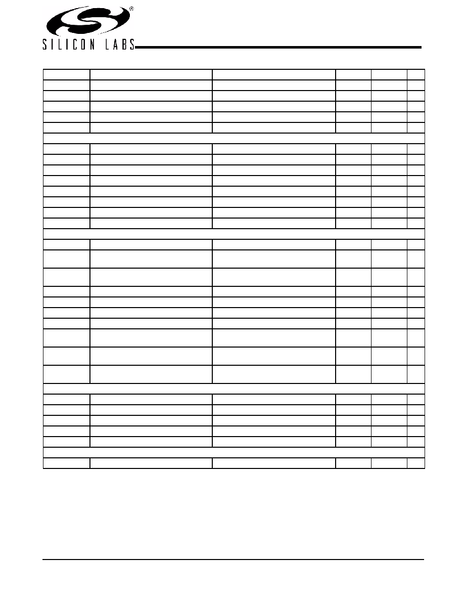
VLOW
Voltage Low
Math averages Figure 9
–150
–
mV
VOX
Crossing Point Voltage at 0.7V Swing
210
550
mV
VOVS
Maximum Overshoot Voltage
–
VHIGH + 0.3
V
VUDS
Minimum Undershoot Voltage
–0.3
–
V
VRB
Ring Back Voltage
See Figure 9. Measure SE
–
0.2
V
PCI/PCIF
TDC
PCI Duty Cycle
Measurement at 1.5V
45
55
%
TPERIOD
Spread Disabled PCIF/PCI Period
Measurement at 1.5V
29.99100
30.00900
ns
TPERIODSS
Spread Enabled PCIF/PCI Period, SSC Measurement at 1.5V
29.9910
30.15980
ns
THIGH
PCIF and PCI High Time
Measurement at 2.4V
12.0
–
ns
TLOW
PCIF and PCI Low Time
Measurement at 0.4V
12.0
–
ns
TR / TF
PCI Edge Rates
Measured between 0.8V and 2.0V
0.89
4.0
V/ns
TSKEW
Any PCI Clock to Any PCI clock Skew
Measurement at 1.5V
–
585
ps
TCCJ
PCIF and PCI Cycle to Cycle Jitter
Measurement at 1.5V
–
500
ps
USB48
TDC
USB Duty Cycle
Measurement at 1.5V
45
55
%
TPERIOD
USB Period,
Measurement at 1.5V, mean value over
1
s
20.8271
20.8396
ns
LACC
Long Accuracy
Measured at 1.5V using frequency
counter over 0.15s
–
100
ppm
THIGH
USB High Time
Measurement at 2.0V
8.094
11.000
ns
TLOW
USB Low Time
Measurement at 0.8V
7.694
11.000
ns
TR / TF
USB Edge Rates
Measured between 0.8V and 2.0V
1.0
4.0
V/ns
TCCJ
Cycle to Cycle Jitter
Measurement taken @1.5V waveform
–
350
ps
TLTJ
Long Term Jitter
Measurement taken from cross point
VOX @ 1 s
–650
ps
TLTJ
Long Term Jitter
Measurement taken from cross point
VOX @ 10 s
–1
ns
TLTJ
Long Term Jitter
Measurement taken from cross point
VOX @ 125 s
–1
ns
REF
TDC
REF Duty Cycle
Measurement at 1.5V
45
55
ns
TPERIOD
REF Period
Measurement at 1.5V
69.827
69.855
ns
TR / TF
REF Edge Rates
Measured between 0.8V and 2.0V
0.55
4.0
V/ns
TCCJ
REF Cycle to Cycle Jitter
Measurement at 1.5V
–
1000
ps
TSKEW
REF Clock to Other REF Clock skew
Measurement at 1.5V
–
500
ps
ENABLE/DISABLE and SET-UP
TSTABLE
Clock Stabilization from Power-up
–
1.8
ms
AC Electrical Specifications (continued)
Parameter
Description
Condition
Min.
Max.
Unit
发布紧急采购,3分钟左右您将得到回复。
相关PDF资料
CY28410OXC-2
IC CLOCK CK410 GRANTSDALE 56SSOP
CY28410OXC
IC CLOCK CK410 GRANTSDALE 56SSOP
CY28411ZXC
IC CLOCK CK410M ALVISO 56TSSOP
CY28442ZXC-2
IC CLOCK ALVISO PENTM 56TSSOP
CY28445LFXC-5
IC CLOCK CALISTOGA CK410M 68QFN
CY28446LFXC
IC CLOCK CALISTOGA CK410M 64QFN
CY28447LFXC
IC CLOCK CALISTOGA CK410M 72QFN
CY28547LFXCT
IC CLOCK CK505/410M INTEL 72QFN
相关代理商/技术参数
CY284108ZXCT
功能描述:时钟发生器及支持产品 Server, CK410B RoHS:否 制造商:Silicon Labs 类型:Clock Generators 最大输入频率:14.318 MHz 最大输出频率:166 MHz 输出端数量:16 占空比 - 最大:55 % 工作电源电压:3.3 V 工作电源电流:1 mA 最大工作温度:+ 85 C 安装风格:SMD/SMT 封装 / 箱体:QFN-56
CY28410OC
制造商:SPECTRALINEAR 制造商全称:SPECTRALINEAR 功能描述:Clock Generator for Intel Grantsdale Chipset
CY28410OCT
制造商:SPECTRALINEAR 制造商全称:SPECTRALINEAR 功能描述:Clock Generator for Intel Grantsdale Chipset
CY28410OXC
功能描述:时钟发生器及支持产品 SysClk Intel Lakeprt & Grantsdale Chipset RoHS:否 制造商:Silicon Labs 类型:Clock Generators 最大输入频率:14.318 MHz 最大输出频率:166 MHz 输出端数量:16 占空比 - 最大:55 % 工作电源电压:3.3 V 工作电源电流:1 mA 最大工作温度:+ 85 C 安装风格:SMD/SMT 封装 / 箱体:QFN-56
CY28410OXC-2
功能描述:时钟发生器及支持产品 SysClk Intel Lakeprt & Grantsdale Chipset RoHS:否 制造商:Silicon Labs 类型:Clock Generators 最大输入频率:14.318 MHz 最大输出频率:166 MHz 输出端数量:16 占空比 - 最大:55 % 工作电源电压:3.3 V 工作电源电流:1 mA 最大工作温度:+ 85 C 安装风格:SMD/SMT 封装 / 箱体:QFN-56
CY28410OXC-2T
功能描述:时钟发生器及支持产品 SysClk Intel Lakeprt & Grantsdale Chipset RoHS:否 制造商:Silicon Labs 类型:Clock Generators 最大输入频率:14.318 MHz 最大输出频率:166 MHz 输出端数量:16 占空比 - 最大:55 % 工作电源电压:3.3 V 工作电源电流:1 mA 最大工作温度:+ 85 C 安装风格:SMD/SMT 封装 / 箱体:QFN-56
CY28410OXCT
功能描述:时钟发生器及支持产品 SysClk Intel Lakeprt & Grantsdale Chipset RoHS:否 制造商:Silicon Labs 类型:Clock Generators 最大输入频率:14.318 MHz 最大输出频率:166 MHz 输出端数量:16 占空比 - 最大:55 % 工作电源电压:3.3 V 工作电源电流:1 mA 最大工作温度:+ 85 C 安装风格:SMD/SMT 封装 / 箱体:QFN-56
CY28410ZC
制造商:SPECTRALINEAR 制造商全称:SPECTRALINEAR 功能描述:Clock Generator for Intel Grantsdale Chipset